In this post we implement the Audio Processor Core logic within our ZedBoard Audio Processor design. The Audio Processor Core is the fourth and final major component in our ZedBoard Audio Processor design’s top level, as mentioned in a previous post.
After debouncing the input buttons and switches on the ZedBoard, generating a master clock signal for the audio codec, and configuring the audio codec via SPI, we are finally ready to start processing audio data. We will do this in the Audio Processor Core.
We configured the audio codec to operate in master I2S mode. I2S stands for Inter-IC Sound, and it describes a serial protocol for transferring digital 2-channel audio. The I2S protocol uses three signals:
- A bit clock, which marks the transfer of every single bit of audio data
- A left/right clock, which indicates the channel to which the information in the data bus belongs
- A data bus, where the audio data is transmitted
The timing diagram for the I2S interface is shown in the figure below.
There are five key takeaways from the timing diagram in the figure above:
- The ADAU 1761 supports a bit depth of 16 to 24 bits per channel, which we configured to 24 bits
- For each sample, the value of the left channel is transferred first, when the left/right clock signal is low
- Both The left/right clock and data signals are shifted at the falling edge of the bit clock
- The data is sampled at the rising edge of the bit clock
- The most significant bit of each sample is shifted one cycle after the left/right clock signal has toggled.
Because the audio codec on the ZedBoard provides both AD and DA conversion, there are two data lines in the I2S interface, though a single instance of SDATA is shown in Figure 1, and both data signals share the same left/right and bit clocks.
The ADAU 1761 uses a two’s complement signed integer format for the audio data, where the MSB is transmitted first. Each 24-bit word can represent an integer value between -8.388.608 and 8.388.607, including the number ‘0‘.
We configured the audio codec to operate in master mode, so both the bit and left/right clock are generated by the codec. The FPGA must ensure that the sampling and shifting of the data happens at the right times with respect to the left/right and bit clock signals.
Though we refer to the left/right and bit clock signals as clocks, they are not ‘actual‘ clocks, meaning that they do not drive any logic within the FPGA. All our logic is driven by the 100 MHz on-board oscillator, whose frequency is several orders of magnitude higher than the audio sampling rate, even if we were working at 96 or 192 kHz. This allows us to treat the left/right and bit clocks as data signals, using the logic driven by the fast 100 MHz clock to oversample them and determine when the edges of the left/right and bit clocks occur. As a result of this, we will never be able to shift or sample data exactly at the edges of the left/right and bit clocks, but we will be close enough to them for our design to work properly. This is a bit of an oversimplification because a complete analysis of the interface timing is outside the scope of this post, but we may cover this at another time.
Zynq Audio Passthrough
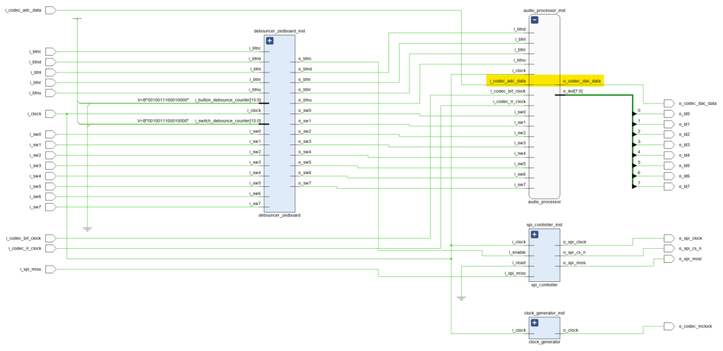
The simplest version of the Audio Processor Core is a passthrough, in which the audio data would literally be passed through from the input to the output. This is shown in the figure below.
As we can see inthe figure above, the ‘i_codec_adc_data’ input signal is wired directly to the ‘o_codec_dac_data‘ output signal, there is no logic between them. This is shown in the code below.
module audio_processor (
    input   logic   i_clock,
    // Audio Interface
    input   logic           i_codec_bit_clock,
    input   logic           i_codec_lr_clock,
    input   logic           i_codec_adc_data,
    output  logic           o_codec_dac_data,
    // Input switches
    input   logic           i_sw0,
    input   logic           i_sw1,
    input   logic           i_sw2,
    input   logic           i_sw3,
    input   logic           i_sw4,
    input   logic           i_sw5,
    input   logic           i_sw6,
    input   logic           i_sw7,
    // Buttons
    input   logic           i_btnu,
    input   logic           i_btnd,
    input   logic           i_btnl,
    input   logic           i_btnr,
    // LEDs
    output  logic [7 : 0]   o_led
);

    timeunit 1ns;
    timeprecision 1ps;

    assign o_codec_dac_data = i_codec_adc_data;

endmodule
The passthrough is great because it allows us to quickly validate what we have done so far. We have actual audio data flowing through our design! At this point you should be able to hear the music that goes in the ‘Line In‘ input of the ZedBoard coming out of the ‘Line Out‘ output, which is already pretty cool.
However, we do want to be able to apply some processing and analysis to the audio data, so we need to go beyond this passthrough. The codec delivers data one bit at a time, so we need to convert the incoming bits into a 24-bit word, which we can use for our processing. And of course, after the las step of processing we need to convert that 24-bit word back to a serial stream of bits that we can send to the audio codec. These tasks will be carried out by the Deserializer and Serializer modules, instantiated at the beginning and the end of the Audio Processor Core. We will discuss those in detail next time.
Cheers,
Isaac


One response to “005 – FPGA Audio Processor Core”
Thank you very much for this tutorial! I followed it and implemented it in VHDL. Works Great!!