In this post, the second in our recurring ‘Paying Off Technical Debt’ series, we will clean up our FPGA Audio Processor design and add support for Vivado’s non-project mode workflow.
The main idea with which I started the FPGA Audio Processor design was to first come up with a working audio passthrough infrastructure (which only requires the Debouncer, the Clock Generator, the SPI Controller and the (De)Serializer modules in the Audio Processor Core) and progressively add all the processing modules that I was interested in exploring. While this sounded great at the time, it has led to the accumulation of technical debt in mainly two ways.
First, the architecture of the design has become increasingly messy, with new modules being added without planning how they will best interact with the rest of the system. There’s a good reason for this: I don’t actually know which modules will be added, or when they will be added, until I decide to start working on them. This isn’t a bad thing, I do want to retain this kind of flexibility. Still, it’s having a negative impact on the design as a whole.
Second, the overhead of managing and processing the entire design has become noticeable over the last few weeks. This overhead was ok at the beginning, when the project was trivially small, but after adding just a handful of modules it has really started to drag things down. This is made worst by a) the fact that I rarely work in more than a single module at a time, and b) working with the Vivado IP Integrator, even though it is not yet needed.
To mitigate both problems at once, I decided to go back to using the basic, purely RTL audio passthrough as the basis for future development. I also included the LED meter because it requires minimal processing and helps a lot with debugging. From now on each new module will be tested in isolation by adding it (and only it) to the passthrough with LED Meter.
Since we are already talking about streamlining the design process, this would be a great opportunity to introduce a non-project workflow for the FPGA Audio Processor, so we will do that as well.
Design Cleanup
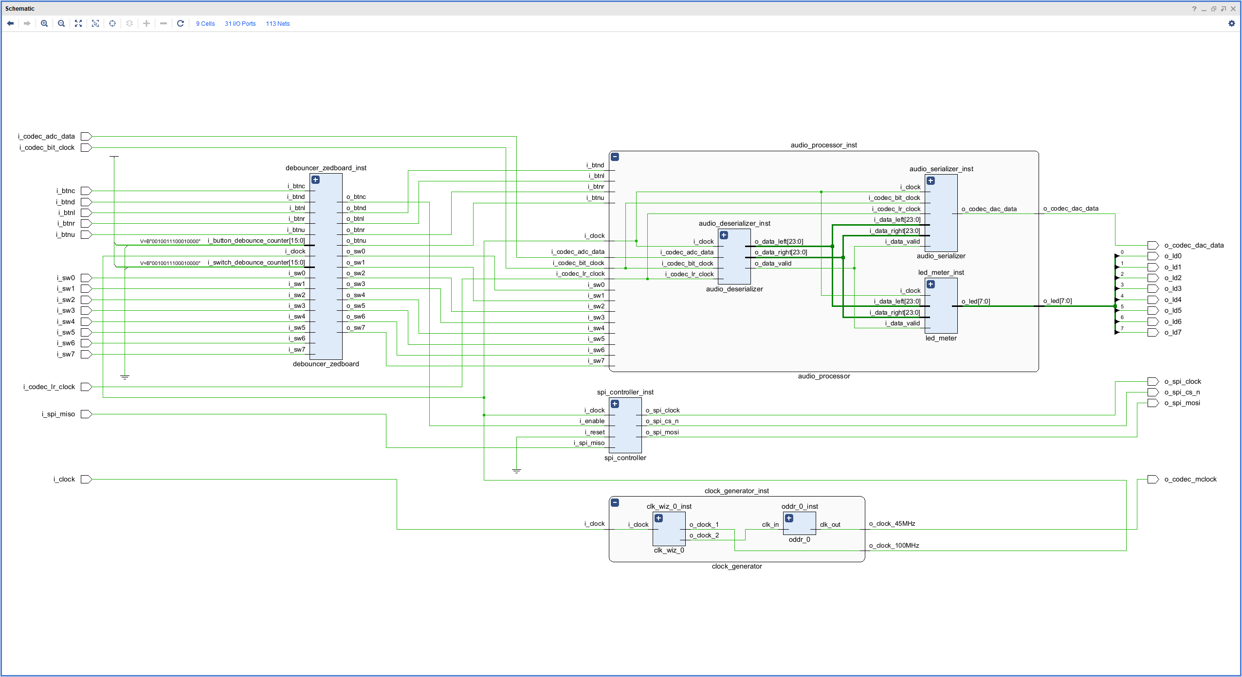
The design cleanup was pretty straightforward: everything that was not needed for the audio passthrough or the LED Meter was removed from the project, including the block design and the Verilog wrappers files. The ‘fpga_audio_processor_top‘ module is back as the project’s top-level unit. The cleaned-up version of the FPGA Audio Processor is shown in the figure below.
Vivado Manage IP Project
Earlier we talked about going back to a purely RTL-based version of the FPGA Audio Processor. This is not entirely accurate, because even after removing the Block Design from the project, we still need to use Xilinx IP in addition to our RTL sources. Because we are switching to a non-project mode workflow, we need to take an extra step here.
When using the non-project workflow, there is not a Vivado project specific to our design with which we can add and customize packaged IP. Xilinx’s recommendation in this instance is to create a so-called Manage IP project. The Manage IP project allows us to customize IP cores independently of a Vivado (non-)project. The xci files generated within the Manage IP project can then be read by our Non-Project Mode script, which we will discuss later.
A Manage IP project can be created by selecting the ‘Manage IP‘ option under the ‘Tasks‘ section of the Vivado start page. The figure below shows the Manage IP project for our FPGA Audio Processor.
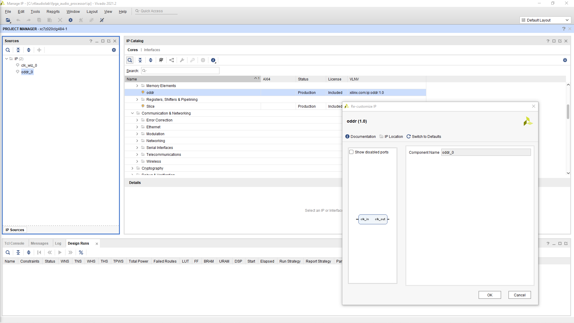
In the Manage IP project we can customize our packaged IP just like we would in a ‘traditional’ Vivado project. We are also able to import existing IP into a Manage IP project, which we did in this case. In this scenario we just need to make sure that the target part or board is the same in the Manage IP and the Non-Project Mode Script (and even in the Vivado project, which we are also keeping).
Non-Project Mode Build Script
When working in non-project mode we interact with the tool via commands. It is possible to use the GUI in non-project mode, but some tasks, especially at the beginning of the process, must be executed using the command line. Because we are not interested in interacting with Vivado on a per-command basis, we can group them into a script that we can run in batch mode. Our non-project build script is based in one of Xilinx’s examples, but has been expanded and cleaned up to support using IP and a more realistic, non-trivial workflow.
# Step 1: define output directory
set output_folder ../output

# Step 2: create in-memory project and define target part
create_project -in_memory
set_property BOARD_PART em.avnet.com:zed:part0:1.4 [current_project]

# Step 3: read design sources and IP files
read_verilog -sv    ../hdl/debounce_fsm.sv
read_verilog -sv    ../hdl/debouncer_zedboard.sv
read_verilog -sv    ../hdl/spi_driver.sv
read_verilog -sv    ../hdl/spi_master.sv
read_verilog -sv    ../hdl/spi_controller.sv
read_ip             ../ip/oddr_0/oddr_0.xci
generate_target {synthesis} [get_files  ../ip/oddr_0/oddr_0.xci]
read_ip             ../ip/clk_wiz_0/clk_wiz_0.xci
generate_target {synthesis} [get_files  ../ip/clk_wiz_0/clk_wiz_0.xci]
read_verilog -sv    ../hdl/clock_generator.sv
read_verilog -sv    ../hdl/audio_deserializer.sv
read_verilog -sv    ../hdl/led_meter_fsm.sv
read_verilog -sv    ../hdl/led_meter.sv
read_verilog -sv    ../hdl/audio_processor.sv
read_verilog -sv    ../hdl/audio_serializer.sv
read_verilog -sv    ../hdl/fpga_audio_processor_top.sv

# Step 4: read synthesis constraints
read_xdc ../constraints/synthesis.xdc

# Step 5: run synthesis, report utilization and timing estimates, write post-synthesis design checkpoint
synth_design -top fpga_audio_processor_top
report_timing_summary -file $output_folder/synthesis/post_synth_timing_summary.rpt
report_power -file $output_folder/synthesis/post_synth_power.rpt
write_checkpoint -force $output_folder/synthesis/post_synthesis_design_checkpoint

# Step 6: read implementation constraints
read_xdc ../constraints/implementation.xdc

# Step 7: run placer and logic optimzation, report utilization and timing estimates, write post-place design checkpoint
opt_design
place_design
phys_opt_design
report_timing_summary -file $output_folder/place/post_place_timing_summary.rpt
write_checkpoint -force $output_folder/place/post_place_design_checkpoint

# Step 8: run router, report final utilization and timing , run drc, write post-route design checkpoint
route_design
report_timing_summary -file $output_folder/route/post_route_timing_summary.rpt
report_timing -sort_by group -max_paths 100 -path_type summary -file $output_folder/route/post_route_timing.rpt
report_clock_utilization -file $output_folder/route/clock_util.rpt
report_utilization -file $output_folder/route/post_route_util.rpt
report_power -file $output_folder/route/post_route_power.rpt
report_drc -file $output_folder/route/post_route_drc.rpt
write_checkpoint -force $output_folder/route/post_route_design_checkpoint

# Step 9: generate bitstream
write_bitstream -force $output_folder/bitstream/fpga_audio_processor.bit
Our Non-Project Mode Script executes through the following steps:
- Step 1 creates a reference to the output directory for the sake of flexibility. We can skip it if wanted to.
- Step 2 creates an in-memory project. This is a seldom-discussed aspect of the non-project mode: Vivado actually creates a minimal project, which only exists in memory. This is required because some of the commands thet we will use later, especially when it comes to IP (and Block Designs, which we are not using for now) require a project to work. After we create the in-memory project we set the target part, or in this case, the target board. This has to match the target part/board of the Manage IP project that was used to create and configure the IP.
- Step 3 reads the design sources and IP files. The ‘read_verilog‘ command with the ‘-sv‘ switch allows us to load our SystemVerilog sources. For each IP we need two steps, one to read the IP configuration file (‘read_ip‘) and another to generate the IP output products to be used in synthesis (‘generate_target‘).
- Step 4 reads the synthesis constraints. We could read all the design constraints at once in this step, but I usually split them into synthesis constraints (which contain the clock and other synthesis-related constraints) and implementation constraints (which contain the IO and other implementation-related constraints).
- Step 5 runs synthesis and generates a set of reports associated with the synthesis process. The non-project mode does not generate any of these reports automatically, so we have to explicitly tell Vivado to create them for us. This step also generates the post-synthesis design checkpoint, which we will discuss later.
- Step 6 reads the implementation constraints.
- Step 7 runs the placement process as well as the pre- and post-placement optimizations. It also generates a timing report and saves the post-place design chekpoint.
- Step 8 routes the design and generates all the (final) reports for timing, utilization and power. It also runs the Design Rules Checker (DRC) and saves the post-route design checkpoint.
- Step 9 generates the bitstream that we will use to program our FPGA.
Design Checkpoints
Our non-Project Mode Script can take a design from source files all the way through to bitstream generation without us having to start the Vivado GUI. However, there are cases in which we would like to interact with the Vivado GUI and do some analysis and checking with the visual tools. This can be achieved with Design Checkpoints.
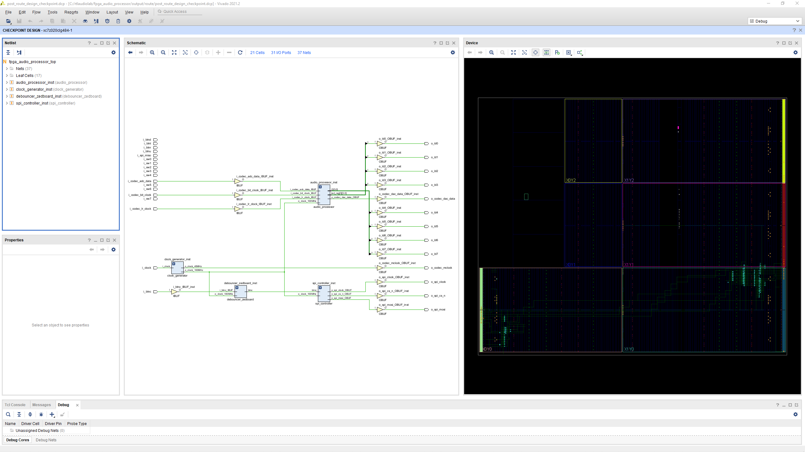
A Design Checkpoint saves the state of a design at a specific point in the workflow. In our script we save checkpoints after synthesis, after placement, and after routing. A Design Checkpoint is a single file with the .dcp extension, and when we open it in the Vivado GUI we get an interface similar to the the one we are used to when working with projects. This is shown in the figure below.
There are several things worth noting when working with design checkpoints:
- The Flow Navigator is not shown, because the Design Checkpoint stores the state of the design at a single stage and does not keep track of what happenned before or what happens afterwards.
- We can use the same analysis tools that we use in project mode, however, we must explicitely save any changes we make to the design or any reports that we generate while working with the GUI.
- Because a Design Checkpoint stores a single snapshot of the design, we lose the ability to cross probe design elements accross stages, like we are used to from the project mode (e.g. selecting an element in the elaborated netlist and following it all the way to the routed design).
Another useful feature of Design Checkpoints is that they allow us to inspect the design at any stage we have previously saved, without having to run synthesis and implementation first.
Vivado Hardware Manager
Now that our Non-Project Mode Script has generated a bitstream file for us, we are ready to program our FPGA. Vivado gives us the option to to start the Hardware Manager without loading a project first, we simply need to select the ‘Open Hardware Manager‘ option under the ‘Tasks‘ section of the Vivado start page. This takes us to the Hardware Manager view with which we are familiar from working in the Project Mode, except there is no project loaded (i.e. no Flow Navigator, no sources, etc.). Here we can connect to our device as usual and program the FPGA with the bitstream generated by our script. This is shown in the figure below.

And that’s it for our design cleanup and non-project setup, at least for now. I’m excited to stick to this workflow for the coming weeks and not have to deal with the Vivado GUI for design entry for the forseeable future. We’ll see how that works and make adjustments when necessary.
Cheers,
Isaac
All files for this post are available in the FPGA Audio Processor repository under this tag. If you would like to support RTL Audio Lab, you can make a one-time donation here.